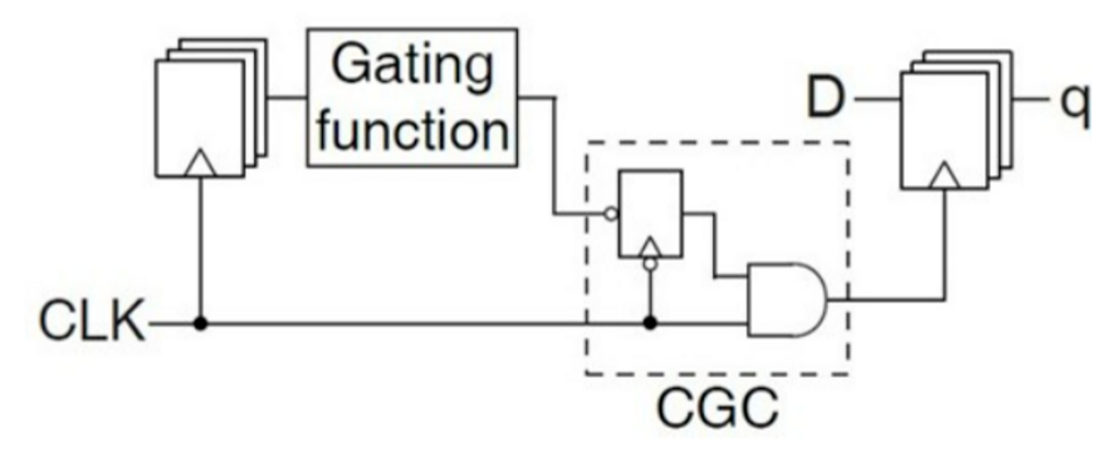
Gate-Level Clock Gating
In sequential cells such as Flip-flop, Clock networks consume more than 40% of the circuit’s total power consumption on average. Therefore, it is important to reduce the power consumption of the clock network for low-power design, and for this purpose, clock gating is used to supply clocks only when the signal of the flip-flop is switched.
We note that a simpler gating function can be derived from a cyclic path that connects the input and output of the same register. A key problem in this approach is to extract a set of cyclic paths of each register, such that power consumption is minimized. We suggest Alogorithm for that problem and simplify the cyclic paths by using don’t care condition and AND/OR gate.
Power Gating Switch Sizing
Power gating is a technique in which a current switch is inserted to reduce leakage current. A circuit is cut off from its power supply in sleep mode by means of a current switch.
When designing a power-gated circuit, it is important to appropriately determine the size of the current switch. The switch must be bigger such that there is no measurable voltage (IR) drop across it. However, in terms of leakage current and area consumption, the smaller the switch, the better. In this work, we aim to derive the optimal size by considering power network and power gating together by using machine learning.

NTV Circuit Design
Near threshold voltage (NTV) circuits are designed to achieve maximum energy efficiency by lowering the operating voltage to near the threshold voltage (Vth). Figure shows the relationship between the operating voltage of the circuit and the energy consumption, showing that the operation at NTV (0.45 V) is 5 times lower than the normal voltage (1.2 V). Thus, NTV circuit design can dramatically reduce critical power consumption in applications such as the Internet of Things (IoT), wearable computers, etc.
However, for NTV circuits, cell delay increases and process error-sensitive drawbacks. Therefore, when designing an NTV circuit, this allows for additional margins, which contributes to increasing the area of the circuit. To address these problems, NTV design methodology studies a methodology that minimizes additional required margins while minimizing power consumption.
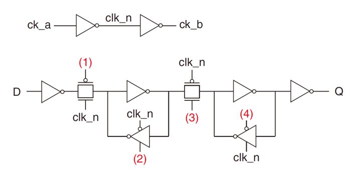
Dual Edge-Triggered Flip-Flop
The current flip-flop used for circuit synthesis is single edge-triggered flip-flop (SETFF), which is only triggered by the charging or falling edge of a clock signal. In contrast, the flip-flop, which is triggered in both rising and falling, is called dual edge-triggered flip-flop (DETFF). If DETFF is used, the frequency of the supply clock can be reduced by half compared to SETFF, which can dramatically reduce clock power consumption. However, the actual DETFF is not being used for circuit synthesis due to problems such as uneven duty ratio of the clock and difficulty in timing analysis.
Therefore, we conducted research on timing analysis methods, clock gating methods and logic simulation for DETFF so that DETFF can be applied to actual circuit synthesis.