IR-DROP PREDICTION
IR-drop is the voltage drop that occurs to reach the Vdd pin of the standard cell in the metal wires that make up the power grid. If IR-drop occurs and the voltage supplied to the standard cell is reduced, the performance of the standard cell can be reduced, resulting in timing violations such as setup violations.
Conventional tool for analyzing IR-drops computes IR-drops by solving a large linear system of equations. But in the case of dynamic IR-drops, the larger the circuit, the more time-consuming it becomes. In this work, we aim to study a model that uses machine learning techniques to quickly predict IR drop.
PDN Synthesis
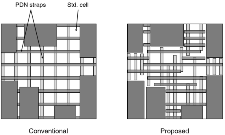
Power distribution network (PDN) is responsible for supplying the current from power pads to standard cells, while satisfying IR-drop constraint.
Conventional PDN synthesis assumes regular PDN straps. Strap widths and pitches are determined in empirical fashion. However, as the wire resistance increases due to technology scaling, PDN requires more power straps. This causes high routing congestion. We aim to study a new PDN synthesis considering routing using machine learning.
3D IC Floorplanning
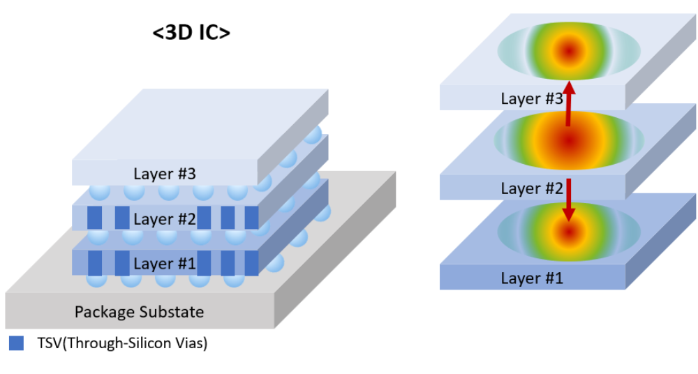
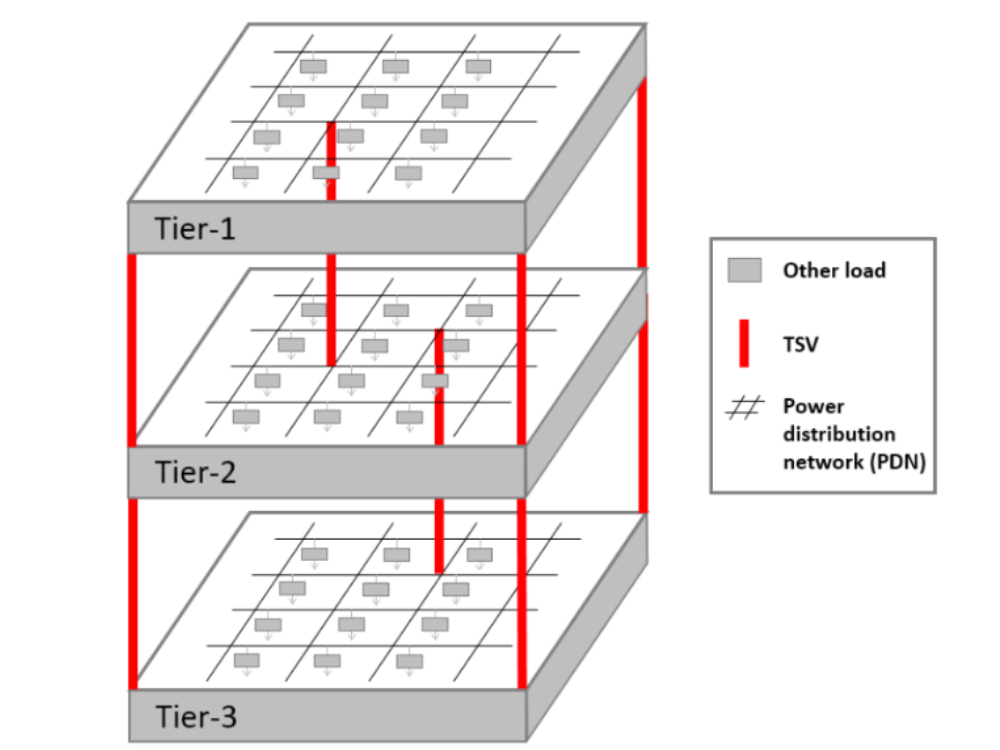
Three-dimensional integrated circuit (3D IC) is a vertical stack of multiple IC layers (as the figure shows). 3D ICs provide higher device density, higher bandwidth, and lower power consumption compared to conventional planar (2D) IC designs.
However, thermal issue is a critical challenge in 3D IC. Vertically stacked multiple layers cause a significant increase in power density. Also, due to low thermal conductivity of dielectric layers, heat generated from the blocks increases the temperature inside the 3D ICs and adversely affects reliability and performance. In order to deal with this thermal issue, thermal-aware 3D IC floorplanning, considering the power consumption and overlapping position of blocks, is necessary.
Our goal is to minimize the chip temperature, while considering other objectives (e.g. chip area, wirelength) based on Machine Learning or Reinforcement Learning.
3D IC PDN Optimization
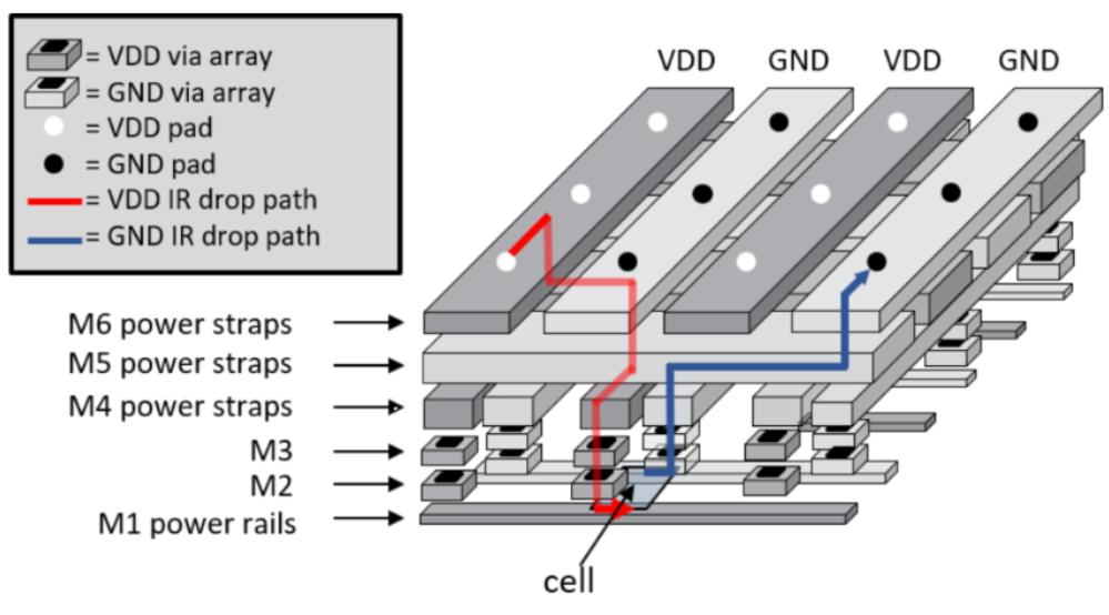
Through silicon via (TSV) is an effective solution in 3D IC because it can reduce the length of global interconnection. However, there are problems with IR drop, thermal dissipation, current delivery per package pin, and various voltage domains among tiers. The design of the power network is very important in 3D IC because it can solve these problems. Traditional 2D design methodology cannot be directly applied to 3D IC because new considerations come into play while optimizing power networks in 3D IC.
First, the number of power/ground IO (PGIO) pads should be limited since one of the major goals in 3D IC is to reduce die area. And placing PGIO in a 2D approach without considering activity between all layers at the same time is not appropriate.
Second, thermal dissipation should be considered by placing the TSV in a location where there is a maximum temperature gradient vertically, not across the layers. PDN is not the only way to reduce the temperature in 3D IC, the placement of the PDN must also consider the TSV for the thermal dissipation path.
Lastly, 2D voltage island partition cannot be applied to 3D layers. This is because power mesh partition and TSV placement must consider all layers.
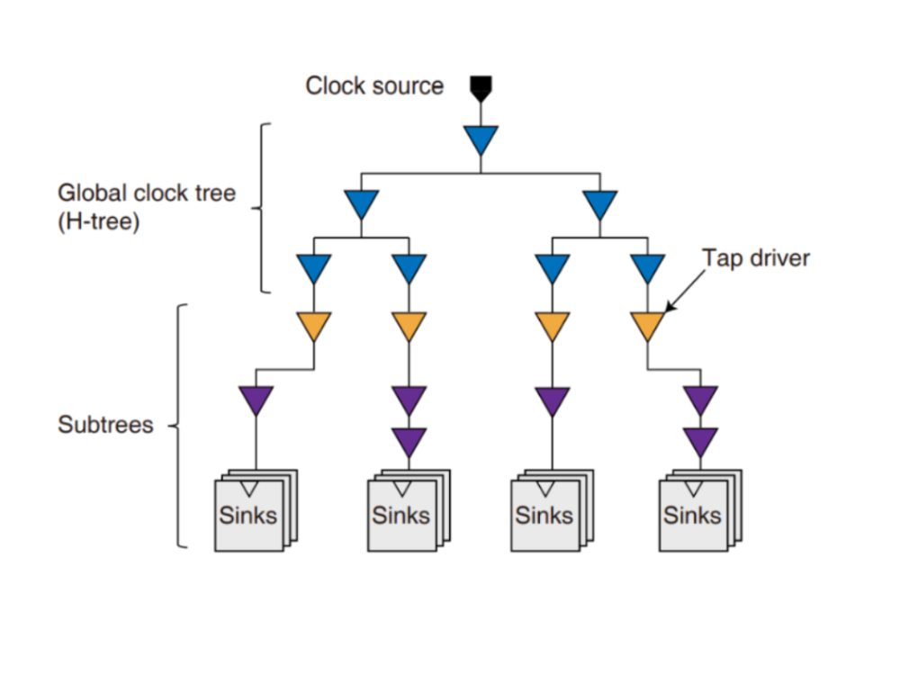
CTS
Clock tree synthesis (CTS) is used to properly assign the external clock to each internal component. Since it needs the location of each component to calculate the exact latency and runnable frequency, CTS must take precedence over signal routing, performed before routing and after placing.
As a clock balancing technique to maintain signal integrity, the common influencing factors are clock uncertainty, clock skew, clock transition and clock latency. The main purpose of our research is to achieve timing convergence by reducing the delay differences on each clock path and minimize the latency.
Analog Layout Automation
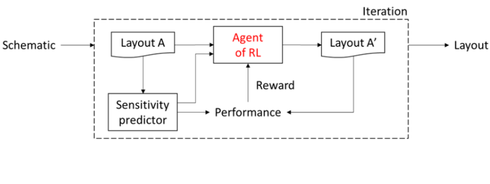
Analog integrated circuits (ICs) play an important role in many system-on-chip (SoC) design applications, such as consumer electronics, bioelectronics, automotive electronics, internet of things (IoT). But electronic design automation (EDA) for the analog IC, especially analog layout design has been a manual, time consuming. We use machine learning to reduce time for designing in this process.
To get a desired specification of layout, designers have to do placement, routing and SPICE simulation many times. We propose a reinforcement learning that can replace the designer’s repetition. Agent receives layout and sensitivity, and trained by performance as reward. After training, agent modifies layout for target specification.