Gate-Level Clock Gating
In sequential cells such as Flip-flop, the clock is used as an input, and therefore a clock network that distributes the clocks entering the circuit to each sequential cell is generated during the circuit synthesis process. Clock networks consume more than 40% of the circuit’s total consumption on average. Therefore, it is important to reduce the power consumption of the clock network for low-power design, and for this purpose, clock gating is widely used to supply clocks only when the signal of the flip-flop is switched.
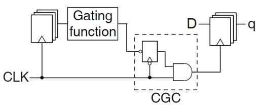
The clock gating method currently used sees the cell’s connection configuration during the RTL phase, and only applies clock gating in (e.g. load-enable register) regions with a specific configuration. Therefore, we study gate-level clock-gating to obtain clock-gating conditions based on the function of each flip-flop at gate-level to solve the problem of limiting flip-flop to which clock-gating is applied.
KEYWORDS Flip-flop, Clock gating
Related Publications Clock gating synthesis of netlist with cyclic logic paths
NTV Circuit Design
Near threshold voltage (NTV) circuits are designed to achieve maximum energy efficiency by lowering the operating voltage to near the threshold voltage (Vth). Figure shows the relationship between the operating voltage of the circuit and the energy consumption, showing that the operation at NTV (0.45 V) is 5 times lower than the normal voltage (1.2 V). Thus, NTV circuit design can dramatically reduce critical power consumption in applications such as the Internet of Things (IoT), wearable computers, etc.
However, for NTV circuits, cell delay increases and process error-sensitive drawbacks. Therefore, when designing an NTV circuit, this allows for additional margins, which contributes to increasing the area of the circuit. To address these problems, NTV design methodology studies a methodology that minimizes additional required margins while minimizing power consumption.
내용 요약 시도 후
Near threshold voltage (NTV) circuits are designed to achieve maximum energy efficiency by lowing the operating voltage. Near threshold voltage (NTV) circuits’ supply voltage is a little larger than threshold voltage. Thus, NTV circuit design has been considered for such applications as IoT where ultra-low power is important.
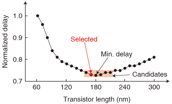
In NTV, a circuit suffers from a large increase in delay and in delay variation. They can seriously affect clock frequency, energy dissipation and circuit area. Figure shows one example of introduced methodology which is optimizing the transistor lengths due to RSCE, to decrease cell delay and delay variation.
KEYWORDS Near threshold voltage
Related Publications Library optimization for near threshold voltage design
Library Optimization through RSCE
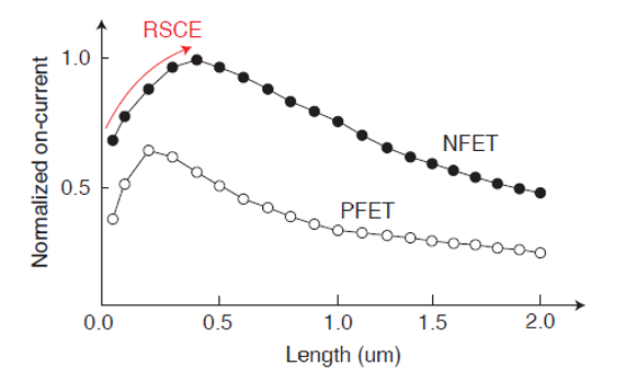
At normal voltage, short channel effect (SCE), such as DIBL or Vth-off, reduces the channel length of the transistor and reduces the Vth. To avoid this, we compensate for the Vth reduction by forming more dopants (halo) on the source and near drain channels. However, on NTV, the SCE is not relatively large due to the low drain voltage, so a small channel length causes a large Vth, which is called reverse short channel effect (RSCE).
Thus, cells of transistor channel length with minimum delay are selected, and cells with the smallest cell size are selected for NTV circuit synthesis.
KEYWORDS Reverse short channel effect
Related Publications Synthesis of dual-mode circuits through library design, gate sizing, and clock tree optimization
Dual Edge-Triggered Flip-Flop
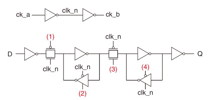
The current flip-flop used for circuit synthesis is single edge-triggered flip-flop (SETFF), which is only triggered by the charging or falling edge of a clock signal. In contrast, the flip-flop, which is triggered in both rising and falling, is called dual edge-triggered flip-flop (DETFF). If DETFF is used, the frequency of the supply clock can be reduced by half compared to SETFF, which can dramatically reduce clock power consumption. However, the actual DETFF is not being used for circuit synthesis due to problems such as uneven duty ratio of the clock and difficulty in timing analysis.
Therefore, we conducted research on timing analysis methods, clock gating methods and logic simulation for DETFF so that DETFF can be applied to actual circuit synthesis.
내용 요약 시도 후
Unlike single edge-triggered flip-flop(SETFF) which is only triggered at the charging or falling edge of a clock signal, dual edge-triggered flip-flop(DETFF) is triggered at both charging and falling edge. DETFF allows us to use whole clock signal while keeping the same throughput. This implies that we can greatly decrease clock power consumption since clock network takes large proportion of total power. However, the DETEF is not being used due to irregular clock H/L ratio and difficulty in timing analysis. In order to solve problems, we propose timing analysis method.
Timing analysis method measures multiple required arrival times(RATs) and then finds the single RAT like dotted region because single RAT can be processed by conventional timing analysis.
KEYWORDS SETFF, DETFF
Related Publications Folded circuit synthesis: min-area logic synthesis using dual-edge-triggered flip-flops